
Equipment Build: Substrate Size Measurement Camera
It has been a while since I’ve put out a site update. I am trying to finish my PhD in a timely manner after all. In the past interval, I’ve spent a fair bit of time building assorted equipment to help with my research, including growth chambers and test/measurement assemblies. I will post articles on the chambers shortly, but just to put something up in the meantime I’ll start with something light that may actually be useful as well (or provide a base for something useful).
1 Overview
Here I present a camera device that uses python/OpenCV to measure the size of pieces of substrate. This has been immensely helpful in the lab as we often scribe larger wafers of Si, MgO, etc, into smaller chunks for test growths in an effort to save money (and the environment? (probably)). If you are careful/lucky, you can break things along cleavage planes and have almost exactly square pieces, but this is not always the outcome. There are certain characterization measurements, e.g. vibrating sample magnetometry (VSM, more on that below), that require knowledge of the film thickness or area. In the example of VSM, the sample total moment is measured, and so the thickness can be calibrated if you know the saturation magnetization and area. This is especially useful when you are growing very thin magnetic films, e.g. < 5 nm, and other methods such as XRR become infeasible. If you are using polished, pre-cut substrates, then this is easy enough, but the area of a randomly cracked shard of substrate is more difficult to determine accurately (before now).
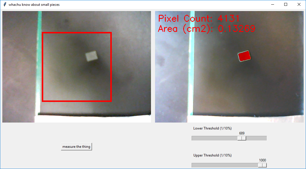
What I’ve created here is a simple and cheap webcam platform to take a snapshot of a substrate on a light or dark background and then integrate the pixels to tell you the area of your piece. After centering your piece in the field of view, you take a snapshot. This snapshot is converted to grayscale and you are presented with two sliders for high and low cutoffs. Moving the sliders back and forth should isolate the area of the substrate piece, and the enclosed pixels are counted. Calibration is done by performing the measurement on a known size of substrate (e.g. 10 mm x 10 mm) and then changing the calibration constant in units of  /pixel.
2 Materials
In regards to hardware, you will need:
- A compatible webcam.
- A rigid stand of some sort.
- A PC with python and assorted packages installed.
- Assorted background materials to place under the substrate.
Most webcams that are advertised as “driverless” (or are linux compatible) should work with the OpenCV API. In this case, I bought a $20 Logitech C170, and removed its housing so I could screw it directly into the stand for rigidity. For the stand, I simply cut 1/16” Al stock by hand and folded it into a trapezoidal stand shape. I removed the camera PCB from its packaging and screwed it directly into this stand, as shown here:
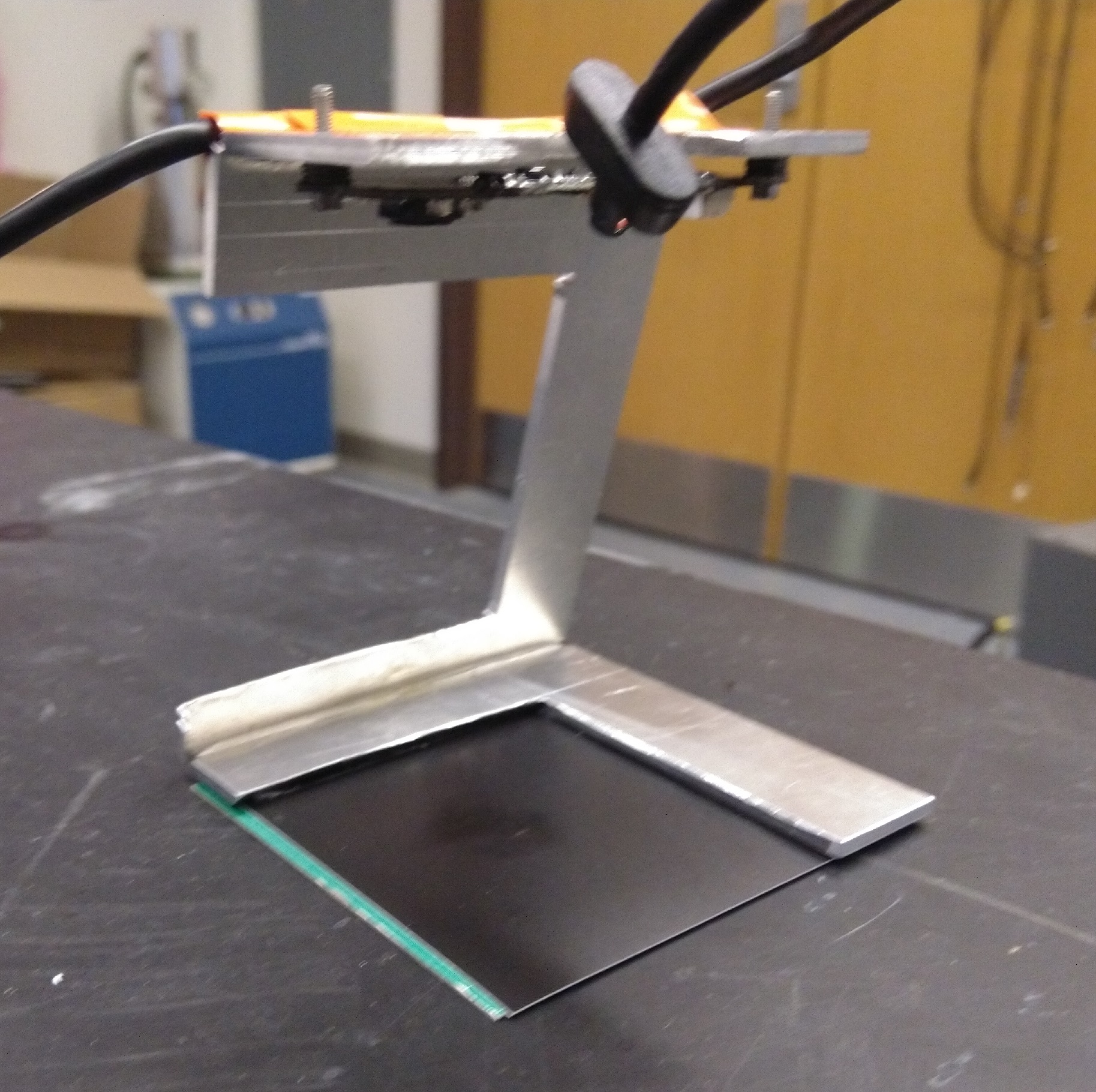
In general, you could probably just make a more simple stand from wood (maybe even actual popsicle sticks, if you think you’re cool enough) and then epoxy the entire camera to it, but I am “particular” so I did what I did. As long as it is relatively stable and the surface is in focus, it should operate just fine with my code.
3 Installation and Operation
Everything here is done with base Python 3.0, with the associated numpy and opencv-python packages. I’ve provided my python script for download here:
Other than installing the dependencies and downloading the script, there are a few user configurable parameters:
FRAME_WIDTH = 1024 #640
FRAME_HEIGHT = 768 #480
AREA_PER_PIXEL = 1.0 # cm^2 / PIXEL NEEDS TO BE CALIBRATED
BURN_FRAMES_COUNT = 1
BOUNDARY_RATIO = 0.6
CAMERA_PORT = 0
These should be changed as follows:
- FRAME_WIDTH/FRAME_HEIGHT: This seems to default to 640x480. You should change it to your camera’s maximum resolution.
- AREA_PER_PIXEL: Conversion constant from pixels to area. Leave as 1.0 for now and calibrate with a known substrate size.
- BURN_FRAMES_COUNT: I noticed some funny behavior when simply snapping the next frame, so I introduced this parameter to burn some frames before saving the final frame for measurement. Leave at 1 and change at your discretion.
- BOUNDARY_RATIO: This sets what section of the total image you want to process, as a ratio of the vertical pixel count. For my setup, I set this at 0.6, which means that a
 pixel square in the center of the frame is being considered with the rest being tossed.
 - CAMERA_PORT: This is not the USB COM port. Cameras are indexed separately. If this is the only camera then the port is 0, with the next port being 1, etc.
To get started, set the camera parameters as desired while leaving AREA_PER_PIXEL = 1.0. Then, load a cut sample of known dimensions into the field of view. Here I have loaded a 10x10 mm sample of MgO:
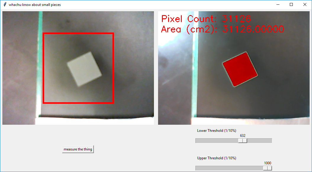
Let’s check that we did a good job by jostling the system around a bit and re-measuring the piece:
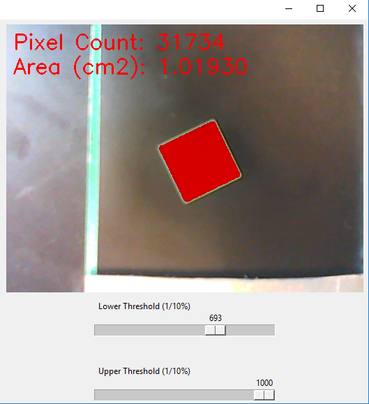
Not bad, a 2% error. I was going very quickly here, and the error can be reduced by setting up a more high contrast background, being more careful with the sliders, etc. The system can also be used in reverse for darker substrates. For a piece of Si, for example, you would put a piece of white paper underneath and do the inverse measurement. The difference between this area and the full area is then the Si shard area.
So in this case, the pixel count of the Si shard is  , giving a Si shard area of approximately
  , which looks right just from visual inspection. Now that the system is calibrated it can be used for practical application.
4 Example Case
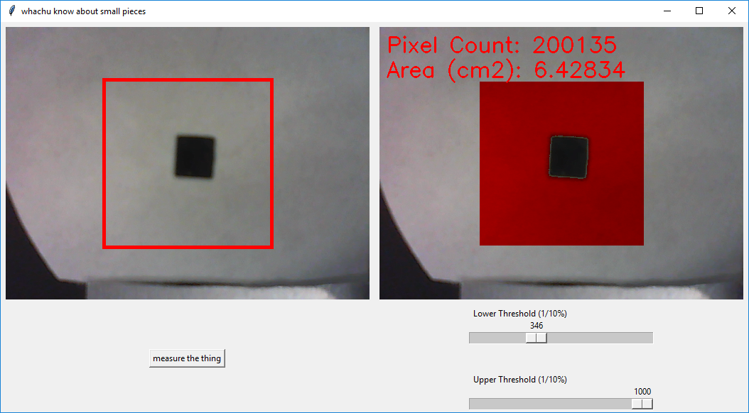
This is an example application, whereby a very thin film of Co is deposited on a tiny shard of Mgo via RF magnetron sputtering (more on that from me later, but here is a link to a decent process description if you’re curious. Because we are  concerned about the environment, we have cut a 5x5 mm MgO substrate into smaller shards for process testing. Here is the shard being used in this growth:
After the Co is deposited, that sample is loaded into the VSM system:
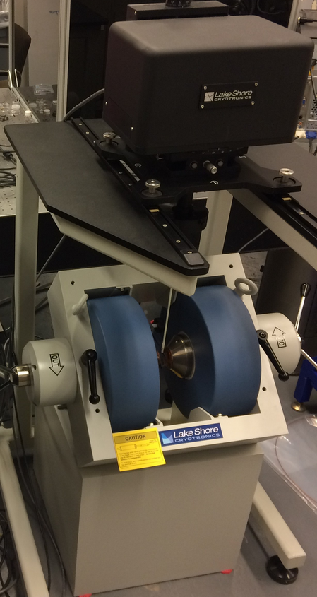
This is a system with large field coils (here up to ~ 2 T) and smaller sensitive pickup coils. The piezoelectric top stage shakes the sample rod up and down at a known frequency (100 kHz typical). The tiny EMF from the magnetic sample induces a current in the pickup coils, which is then amplified and measured. In this case, the Co was grown to a thickness of several nanometers, so we would expect full in-plane anisotropy (a nice square loop in-plane). Indeed this is what was captured:
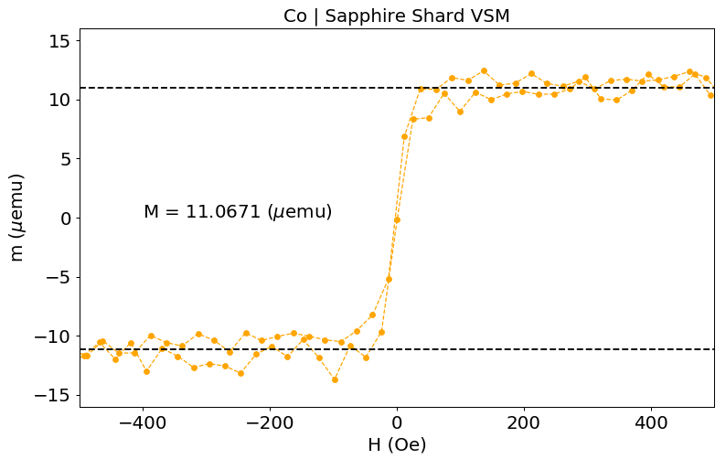
From the loop amplitude, and assuming a bulk saturation magnetization  :
:

We were aiming for a 1 nm film here, and this is in the expected range. This information would then be used to infer conditions about growing thinner or thicker films. If we wanted to try for something closer to exactly 1 nm, for example, we would increase the deposition time by about 60%.
The analysis here is slightly simplified. In the ultra thin film limit, which this is, strain transfer from the substrates changes the intrinsic properties significantly. From assorted literature,  is probably in the range
 ![[1000,1300] (emu/cm^3)](https://www.stevenovakov.com/texcache/29562547e3bd4c00c33b40519fa13fbfe3e28b6di.svg) for a film of this thickness, which would give a more likely range of [0.65, 0.85] (nm) for the thickness. Astute readers might ask whether the film is continuous. In this case, AFM data, as well as the cleanliness of the in-plane loop suggest that it probably is.
for a film of this thickness, which would give a more likely range of [0.65, 0.85] (nm) for the thickness. Astute readers might ask whether the film is continuous. In this case, AFM data, as well as the cleanliness of the in-plane loop suggest that it probably is.
5 Conclusion
There it is, a little camera unit to tell you the size of your substrate shards and help with accurate characterization of your film. Now you can cut everything haphazardly and have the computers measure the thing for you #thefutureisnow. If I was more cool than I am right now, I would train some sort of edge detection scheme to find the substrate automatically, but this is fast enough by hand and so that’s not really necessary, in my opinion.